KiCad Tutorial: Designing a Simple LED Circuit
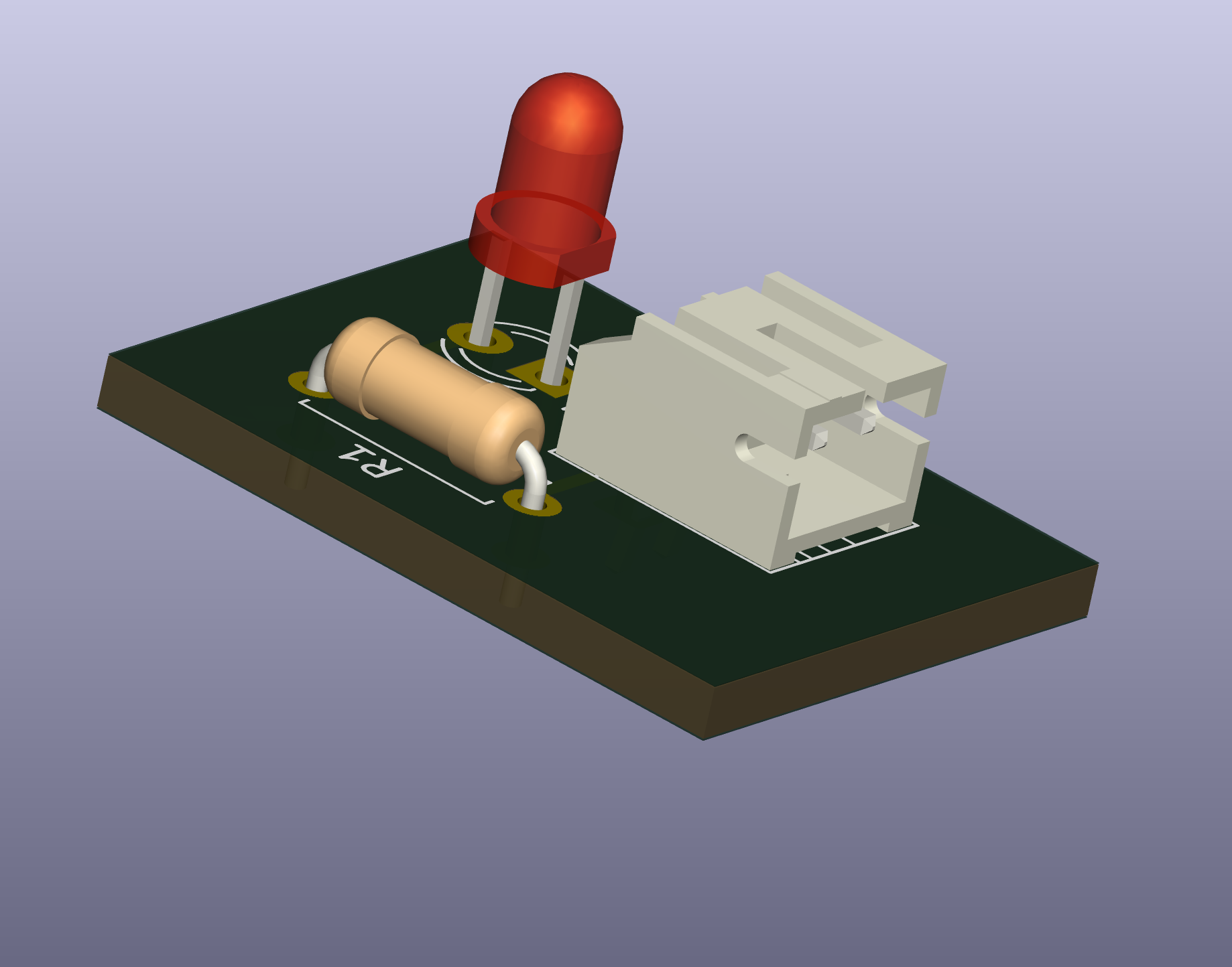
We used KiCad for creating a PCB with a simple LED circuit powered by a 3.7V LiPo battery connected via a JST-PH connector. We begin with creating a scheamtic file, then generating a 3D render and exporting the files necessary to produce the PCB.
Schematic Layout
Initially we placed symbols JST connector (J1), resistor (R1), and LED (D1) to the schematic and then assigned footprints to it:
- JST Connector (J1) Connector_JST:JST_PH_S2B-PHK_1x02_P2.00mm_Horizontal
- Resistor (R1) Resistor_THT:R_Axial_DIN0207_L6.3mm_D2.5mm_Horizontal
- LED (D1) LED_THT:LED_D3.0mm
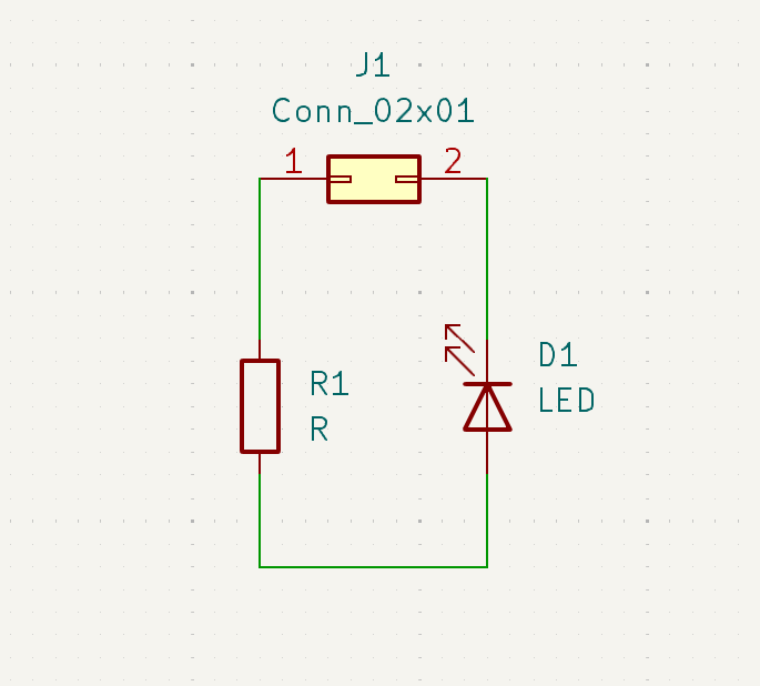
After that wire connection was established between the components accordingly. Then we “Annotate Schematic” and “Perform ERC” to check for errors.
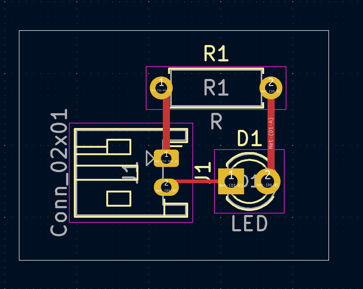
PCB Layout
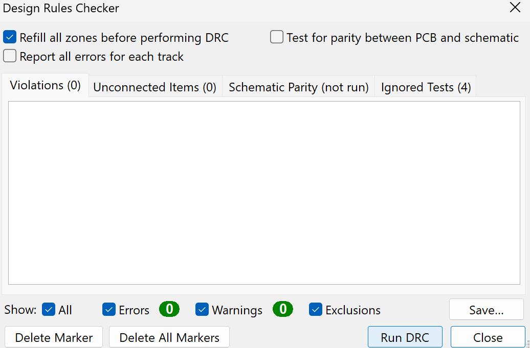
On clicking “Update PCB from Schematic” or using Shortcut: F8 all footprints will be imported. Components are closely placed and an outline box is created using “Edge.Cuts”. Tracks are routed on the board and for analysis, “Design Rules Check (DRC)” was run and come back with zero errors.
3D View